
Contents
- 1 1. The Invisible Battlefield of Modern Technology
- 2 2. Why Traditional PCB Processing Is Quietly Failing
- 3 3. Laser Processing: Not an Upgrade, but a Paradigm Shift
- 4 4. PCB Laser Marking: From Labels to Digital Identity
- 5 5. “Cold Processing”: The Silent Advantage of UV Lasers
- 6 6. Beyond Marking: A Full Laser Ecosystem
- 7 7. Automation: Where Real Value Emerges
- 8 8. Breaking the Industry’s Biggest Illusion
- 9 9. Final Insight
1. The Invisible Battlefield of Modern Technology
Printed Circuit Boards (PCBs) are not components—they are infrastructure. Every smartphone, EV, medical device, and satellite depends on them. As devices shrink and functionality explodes, PCB complexity is increasing at an exponential rate.
Modern data shows:
- PCB feature sizes are moving toward micron-level precision
- Component density has increased by over 300% in the last decade
- Failure tolerance is approaching near-zero in high-end electronics
This creates a brutal reality:
traditional manufacturing methods are no longer sufficient.
2. Why Traditional PCB Processing Is Quietly Failing
Historically, PCB production relied on:
- Mechanical routing
- Die punching
- V-scoring
These methods still exist—but they come with structural limitations:
- Tool wear reduces consistency
- Mechanical stress damages micro-components
- Burrs and edge defects reduce yield
As highlighted in industrial practice, these limitations are becoming more critical as PCB designs evolve toward high-density interconnect (HDI) architectures.
The conclusion is unavoidable:
mechanical precision cannot keep up with electronic miniaturization.
3. Laser Processing: Not an Upgrade, but a Paradigm Shift
Laser technology introduces a fundamentally different manufacturing philosophy:
- Non-contact processing → zero mechanical stress
- Ultra-fine beam control → micron-level accuracy
- High-speed automation → scalable production
Unlike traditional tools, lasers interact with material through energy—not force. This eliminates deformation while enabling extremely fine processing.
For example:
- UV laser beam diameter can reach ~20 μm
- Minimal heat-affected zones prevent component damage
This is not incremental improvement—it is manufacturing at the scale of electrons.
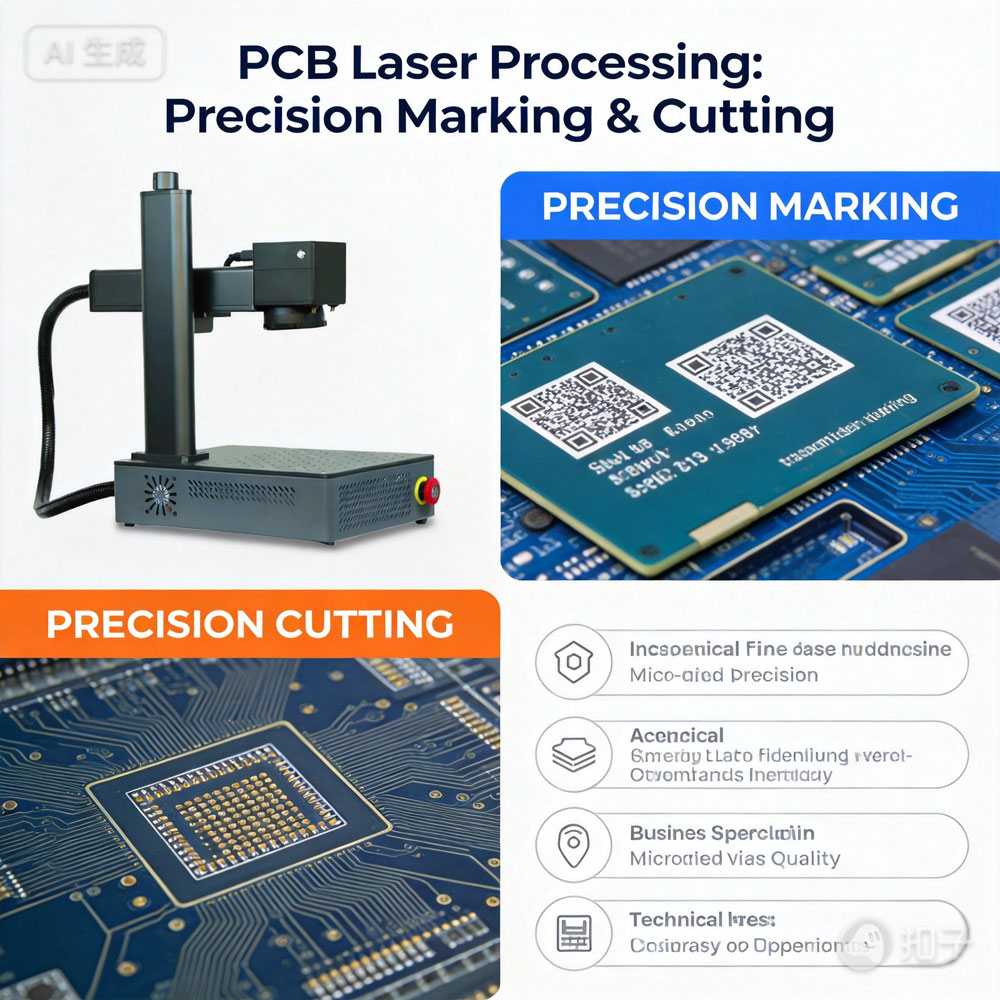
4. PCB Laser Marking: From Labels to Digital Identity
One of the most underestimated applications is PCB laser marking.
Laser systems can create:
- Serial numbers
- QR / Data Matrix codes
- Logos and micro-text
- Anti-counterfeiting patterns
These markings are:
- Permanent
- High-contrast
- Resistant to environmental stress
More importantly, they enable full lifecycle traceability.
Each PCB becomes a data carrier, linking:
- Production batch
- Process parameters
- Quality inspection data
This transforms marking from a cosmetic step into a data architecture layer.
5. “Cold Processing”: The Silent Advantage of UV Lasers
A critical breakthrough lies in UV laser technology.
Unlike traditional thermal methods:
- UV lasers use a “cold marking” approach
- Minimal thermal diffusion
- No damage to surrounding materials
This is essential for:
- Flexible PCBs (FPC)
- Semiconductor-level components
- Heat-sensitive substrates
In practical terms:
you can process fragile electronics without touching their structure.
6. Beyond Marking: A Full Laser Ecosystem
Laser technology in PCB manufacturing is not limited to marking. It extends to:
Laser Depaneling
Clean separation of PCBs without stress or burrs
Laser Drilling & Cutting
Ultra-precise microvias and complex geometries
Laser Decoating
Efficient removal of glue or coatings with high accuracy
Compared to manual or chemical processes, laser decoating:
- Improves yield
- Reduces contamination
- Increases speed significantly
This creates a unified ecosystem where one technology replaces multiple legacy processes.
7. Automation: Where Real Value Emerges
Modern PCB laser systems are not standalone machines—they are production nodes.
Key capabilities include:
- Inline integration (SMEMA-compatible systems)
- CCD vision positioning and verification
- Real-time code reading and inspection
- Automated conveyor-based workflows
This enables:
- Lights-out manufacturing
- Zero human error marking
- Scalable high-volume production
The shift is clear:
from machines to intelligent manufacturing systems.
8. Breaking the Industry’s Biggest Illusion
Most manufacturers still think:
“Laser improves PCB processing.”
That is too small.
The real transformation is:
Laser redefines what is manufacturable.
Without laser:
- Ultra-dense PCBs are unreliable
- Traceability is incomplete
- Yield drops under complexity pressure
With laser:
- Micro-scale precision becomes standard
- Data becomes embedded into hardware
- Production becomes digital-first
9. Final Insight
PCB laser processing is not about better cutting or marking.
It is about aligning manufacturing with the scale, speed, and intelligence of modern electronics.
As electronics continue to shrink and systems become smarter, one truth becomes unavoidable:
The future of hardware will be written with light.