
Home › Forums › Laser Marking Forum › Laser Marking for IC Chips: Building Traceability in the Semiconductor Age
- This topic is empty.
-
AuthorPosts
-
03/26/2026 at 10:28 PM #886
Dwmin
Keymaster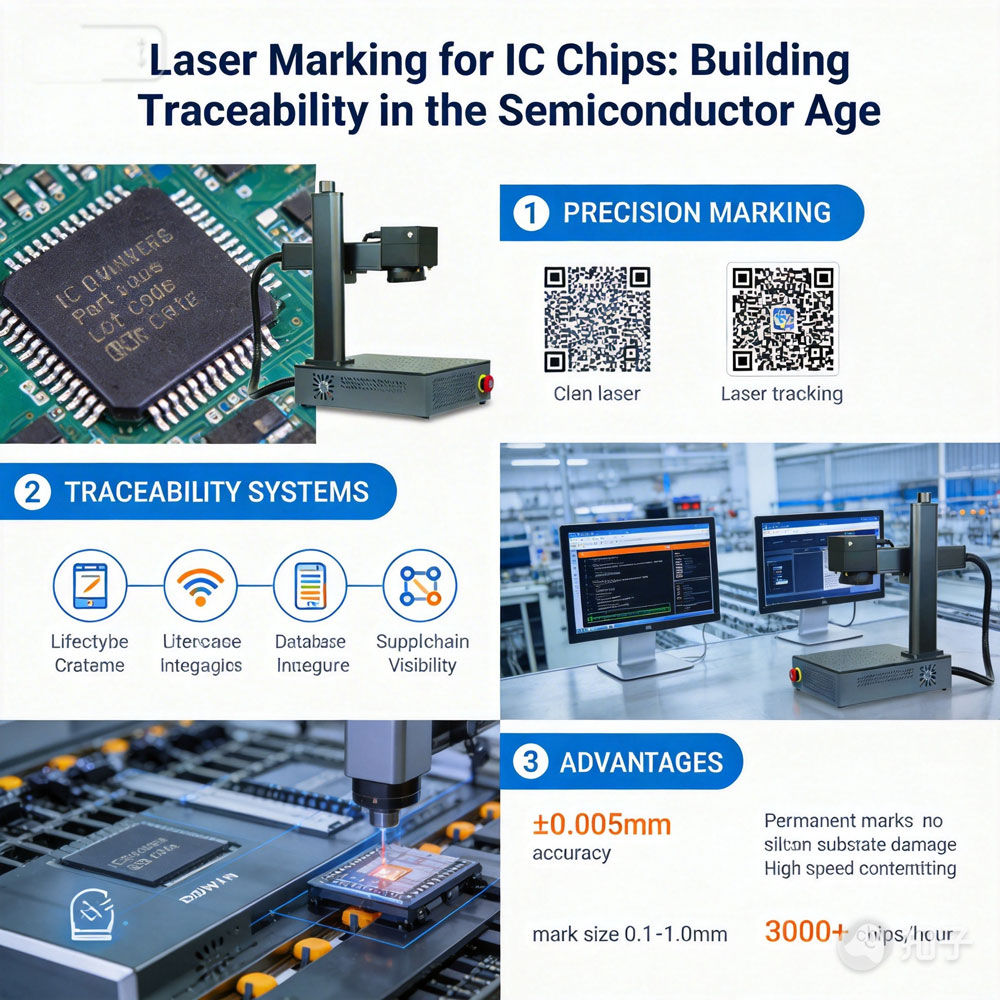
1. The Semiconductor Industry Has a Visibility Problem
Modern semiconductors are everywhere—AI servers, smartphones, vehicles, medical systems. Yet behind this technological explosion lies a critical challenge:
How do you track something you can barely see?
IC chips are:
- Microscopic in size
- Mass-produced at extreme volumes
- Distributed across complex global supply chains
Industry data indicates that a single chip may pass through dozens of process steps and multiple facilities before reaching final assembly. Without reliable identification, traceability collapses.
This is why marking is no longer optional—it is foundational to semiconductor manufacturing.
2. Why Traceability Is Non-Negotiable
In semiconductor production, every chip must carry a unique identity for three core reasons:
- Quality control and defect tracking
- Anti-counterfeiting and authenticity verification
- Regulatory and supply chain compliance
Laser marking enables chips to carry:
- Serial numbers
- DataMatrix or QR codes
- Batch and production information
These markings allow manufacturers to trace each component from wafer to final product, ensuring full lifecycle visibility.
3. Why Traditional Marking Methods Failed
Older marking methods—ink printing, mechanical engraving—simply cannot meet semiconductor requirements:
- Insufficient resolution for micro-scale surfaces
- Risk of contamination in cleanroom environments
- Poor durability under heat and chemical exposure
Semiconductor manufacturing demands:
- Micron-level precision
- Zero contamination
- High-speed throughput
Only laser technology satisfies all three simultaneously.
4. How Laser Marking Works on IC Chips
Laser marking uses a focused beam of light to modify the chip surface without physical contact.
Key characteristics:
- Non-contact process → no mechanical damage
- High-energy beam → precise material interaction
- Permanent marking → resistant to wear and chemicals
The laser creates marks by:
- Localized heating
- Surface ablation
- Chemical or structural modification
The result is a high-contrast, permanent identifier at micro-scale resolution.
5. Precision at the Micron Level
IC chips are extremely small, with dense packaging formats such as:
- SOP
- QFN
- LGA
- BGA
This requires:
- Ultra-fine beam control
- Accurate positioning systems
- Minimal heat-affected zones
Modern systems can achieve alignment accuracy within tens of microns, ensuring readable and consistent codes even on tiny surfaces.
This level of precision is not optional—it is the baseline for semiconductor manufacturing.
6. From Marking to Intelligent Inspection
Laser marking systems today are no longer standalone tools—they are integrated inspection platforms.
Advanced capabilities include:
- Vision systems detecting misalignment or missing marks
- Real-time defect identification
- Automated correction and feedback loops
This transforms marking into:
A quality control checkpoint, not just a labeling step.
7. Full Automation: The Real Productivity Driver
Semiconductor production is high-volume and high-speed. Manual processes are impossible.
Modern laser marking systems support:
- Fully automated loading/unloading
- Dual-lane conveyors for continuous flow
- Recipe-based switching for different chip types
- Integration with MES, EAP, and SECS/GEM systems
This enables:
- High-mix, high-volume manufacturing
- Reduced human error
- Scalable production efficiency
8. The Hidden Advantage: Cleanroom Compatibility
Semiconductor fabrication environments demand extreme cleanliness.
Laser marking offers:
- No ink or chemical consumables
- No particle generation
- No physical contact
This makes it inherently compatible with cleanroom standards, unlike traditional marking methods.
9. The Bigger Picture: Data Embedded in Silicon
The industry still tends to view marking as identification.
That is outdated.
Today, each marked chip becomes:
- A data node
- A traceability anchor
- A digital interface between physical and information systems
From wafer-level IDs to final package codes, laser marking ensures that every chip can be tracked across:
- Manufacturing
- Testing
- Assembly
- Deployment
10. Breaking the Industry’s Old Assumption
Old mindset:
“Marking is just labeling.”
New reality:
Marking is data infrastructure.
Without reliable marking:
- Defect tracing becomes impossible
- Supply chain transparency collapses
- Counterfeit risks increase
Laser marking is not a supporting process—it is central to semiconductor intelligence.
11. Final Insight
As chips become smaller and more complex, the importance of marking increases—not decreases.
Because:
The smaller the device, the more critical its identity.
Laser marking enables something fundamental:
- Turning invisible components into traceable, verifiable, and intelligent assets
The future of semiconductors will not only be defined by processing power.
It will be defined by this:
How well every chip can be identified, tracked, and trusted.
-
AuthorPosts
- You must be logged in to reply to this topic.